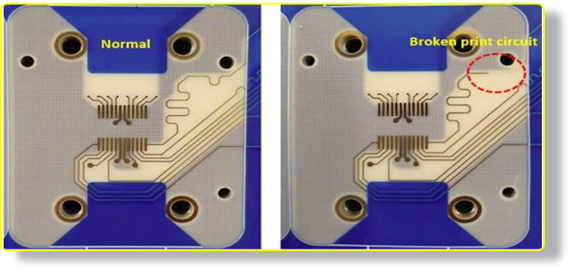
PCB SUBSTRATE LEVEL REPAIR & RESTORATION

  • Loadboard & test pads restoration(PROPRIETARY)
  • Restore damaged component
  • Restore damaged copper traces
  • Repair and restore burnt PCB substrate
  • Restore solder mask
  • TEST PADS MODIFICATION

  • Test Pads extension
  • Test Pads re-alignment/ centering
  • Rectify wrong copper trace links
  • TEST PADS RESTORATION: DURAPAD & DURAPAD+ Technology

  • Damaged by POGO Pin or Johnstech
  • Hi-temp & high current application
  • Hard gold plating finish
  • HARDWARE

  • PEM nuts, Pins, receptacles, & component change
  • Sockets & connector extract & install - SMD/ PTH
  • Safe PCB wash - flux, soil and other contaminants cleaning
  • COPPER TRACES

  • Broken copper traces/ jumpers
  • SMD pads, annular rings, barrels restoration
  • DOA

    Dead or Alive

    AOD

    Alive on Delivery

    Before Repair

  • Damaged PTH & annular rings
  • Damaged copper traces & OPEN connections.
  • After Repair

  • Restore PTH and annular rings
  • Replace jumper wires
  • Restore broken copper traces
  • Before Repair

  • Damaged SMD pads due to improper de-soldering
    of component.
  • After Repair

  • Restored all missing component pads
  • Check all connections
  • Before Repair

  • Broken/ missing RF signal trace
  • After Repair

  • Restored Broken/ missing RF signal trace
  • Copy exact dimension of trace lines from other sites
  • OUR TECHNOLOGY
    (TWO RESTORATION
    METHODOLOGIES)

    - DURAPAD① restoration technology 375 Knoop hardness /
    up to 125 °C Test Temp
    - DURAPAD+ restoration technology 375 Knoop hardness /
    up to 165 °C Test Temp
  • 50u” Hard gold over 200u” nickel finish
  • Multi-site planarity / flat surface
  • No contaminants between pads to cause leakage
  • HIGH Current test capable
  • CURRENT INDUSTRY
    PRACTICE

  • Copper strip soldered over damage copper
  • 50u” Hard gold over 200u” nickel finish
  • Planarity of test pad surface between sites is a challenge
  • May induce contaminants (adhesive & flux)
    between pads to cause leakage
  • Before and After Restoration using our Technology

    1 / 14
    BEFORE
    2 / 14
    AFTER
    3 / 14
    BEFORE
    4 / 14
    AFTER
    5 / 14
    BEFORE
    6 / 14
    AFTER
    7 / 14
    BEFORE
    8 / 14
    AFTER
    9 / 14
    BEFORE
    10 / 14
    AFTER
    11 / 14
    BEFORE
    12/ 14
    AFTER
    13 / 14
    BEFORE
    14 / 14
    BEFORE

    What is special about our capability?

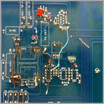
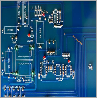
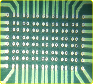
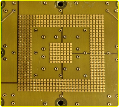
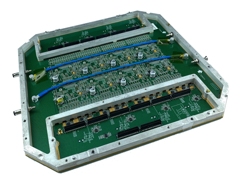
    -Shortest delivery turn-around time for Loadboard test pads restoration.

  • 3-day leadtime on complex restoration jobs.(Multi- site/ high pad count, with over 1000 pads)
  • 24 hour expedite repair time on urgent requirement.
  • Within-the-day delivery with HOUSE CALL.
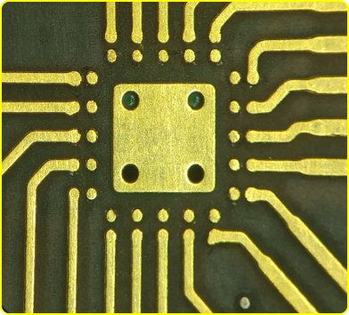
  • --Proven durability with longer tool life, more insertion.

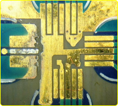
    ---Passed Analog, Mixed-signal and RF application.

    NEED FOR SPEED?

  • 24-hour express delivery for Loadboard test pads repair and restoration.
  • House call - 8-hour express repair service to bring your test loadboard back in production quickly. Our service personnel will visit your factory and repair your board at site.