EXISTING PCB MODIFICATION & CIRCUIT CORRECTION
PTH to VIP conversion
Add missing copper traces
Circuit correction or trace modification
Test pad extension/ modification
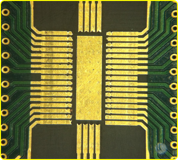
HIGHLIGHTS: PTH to Blind VIA conversion
To correct design error in PTH drill size.
Silver fill all Plugged thru holes.
Maintain test pads planarity.
Restore plating finish - 50 u” Au over 200 u” Ni.
NOTE: added copper trace lines are ~ 4mils thick
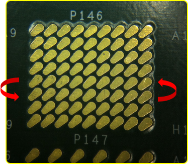
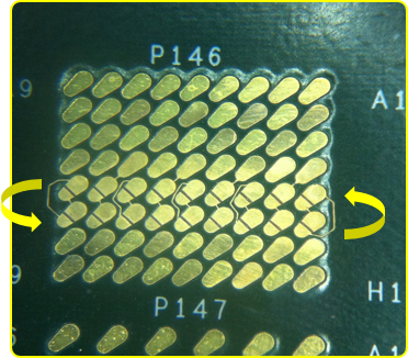
HIGHLIGHTS: BGA Pads inter-connect correction
Wrong pad connections - a design error.
Interchange pad connections.
All pads planarized to maintain level across all pads.
Restore plating finish - 50 u” Au over 200 u” Ni.
HIGHLIGHTS: Test Pads extension
Extend test pads to center pogo pin hit area.
Maximum pad gap to center pad is 0.25mm.
Maintain test pads planarity.
Restore plating finish - 50 u” Au over 200 u” Ni.
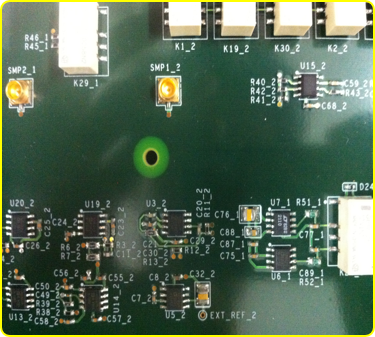
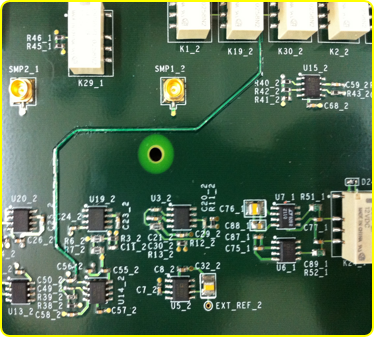
HIGHLIGHTS: Add missing copper trace connection
Add Point-to-point signal route connection
Use of copper trace instead of jumper wire.
Solder mask to cover added copper trace
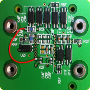
HIGHLIGHTS: Add copper trace connection.
Add Point-to-point signal route connection.
Use of copper trace to connect instead of jumper wire.
Solder mask cover added over copper trace.